

Key Takeaways
- Nanometer numbers describe manufacturing process sophistication, not a precise physical size.
- Smaller nodes pack more transistors onto a chip, boosting speed and reducing power draw.
- The race to 2nm is driven by demand for AI, mobile, and data center performance.
- Achieving smaller nodes requires extraordinarily expensive and complex manufacturing equipment.
- Geopolitical control over advanced chip manufacturing has become a major strategic concern.
2-Nanometer Chip Node
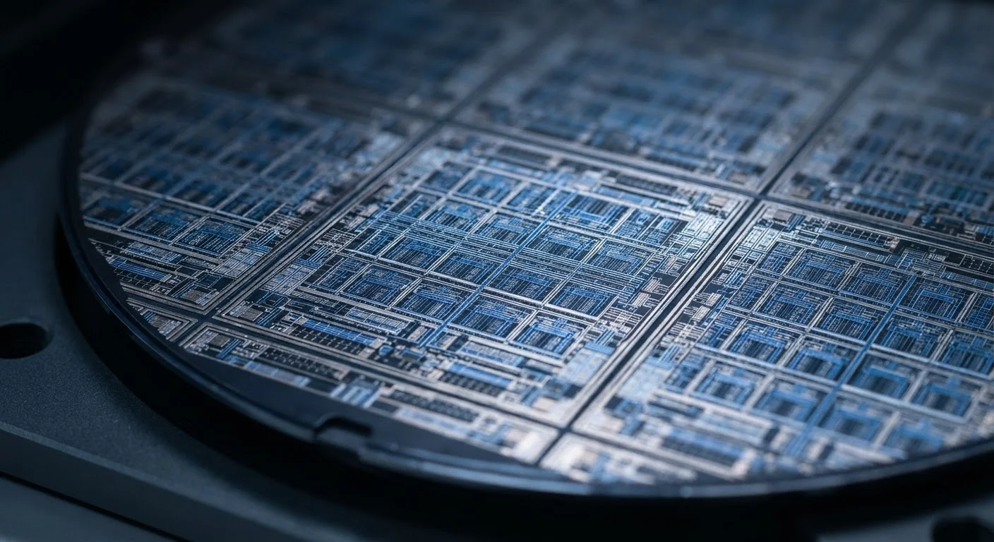
A 2-nanometer chip refers to a semiconductor manufacturing process in which transistors - the tiny on/off switches that power computing - are built at an extremely small scale. The label describes the density and sophistication of the manufacturing process rather than a literal physical measurement. Smaller process nodes generally allow more transistors to fit on a single chip, enabling faster performance and lower energy use.
The 'nanometer' branding used by chipmakers is a marketing convention, not a strict dimensional standard. Actual gate lengths and feature sizes differ by manufacturer and do not correspond directly to the stated node number.
What the Numbers Actually Mean
When chipmakers announce a new nanometer milestone, the number sounds precise - almost scientific. In practice, it functions more like a generation label than a measurement. A nanometer is one-billionth of a meter; a human hair is roughly 80,000 nanometers wide. So "2nm" describes transistors operating at a scale that dwarfs most biological structures.
The confusion arises because the industry stopped using nanometer figures as direct physical measurements around the early 2010s. Today, the number signals where a process sits in a sequence of increasingly sophisticated manufacturing generations. What matters is what that generation delivers: how many transistors fit on a given area of silicon, how fast they switch, and how much energy they consume doing it.
Understanding chip architecture fundamentals can help explain why transistor density isn't the only variable - design philosophy matters just as much as manufacturing precision.
Why Smaller Translates to Better
Each new process node aims to achieve three things simultaneously: higher performance, lower power consumption, and reduced cost per transistor. Packing more transistors into the same silicon area means a chip can do more work without growing physically larger or drawing more electricity.
This matters enormously for mobile devices, where battery life is a constant constraint, and for data centers, where power consumption translates directly into operating costs. It also matters increasingly for AI workloads, which are computationally intense. As the push for efficient AI models accelerates, the hardware underneath needs to keep pace.
~100B
Transistors in advanced modern chips
Leading-edge processors announced in recent years contain transistor counts in the tens to hundreds of billions, illustrating the density gains from successive process nodes.
$20B+
Typical cost to build a leading-edge fab
Industry analysts estimate that constructing a state-of-the-art semiconductor fabrication plant requires capital investment exceeding twenty billion dollars.
~30%
Typical power efficiency gain per node
Semiconductor researchers generally cite efficiency improvements in the range of 25-35% when moving between major process node generations, though gains vary by design.
The gains from each new node are real but diminishing. Moving from 7nm to 5nm delivered substantial improvements; the jump from 3nm to 2nm is harder won and more expensive to achieve, requiring new materials, new lithography techniques, and entirely redesigned manufacturing workflows.
The Manufacturing Complexity Behind the Headlines
Building chips at 2nm requires extreme ultraviolet (EUV) lithography - a process that uses light with a wavelength shorter than any previously used in chip production to etch transistor patterns into silicon. The machines capable of this cost hundreds of millions of dollars each and are produced by only one company globally. The supply chain for these tools is itself a geopolitical pressure point.
EUV Lithography: A Single-Source Dependency
Extreme ultraviolet lithography machines - essential for manufacturing chips at 3nm and below - are produced by a single Dutch company. Every leading chipmaker worldwide depends on this supply. Export control policies targeting these machines have made them one of the most strategically sensitive pieces of industrial equipment on earth.
Chip fabrication plants, known as fabs, take years and tens of billions of dollars to build. A production-ready 2nm fab represents one of the most capital-intensive industrial investments a company can make. This explains why advanced chip manufacturing is concentrated in a very small number of locations worldwide - a vulnerability that became starkly visible during recent semiconductor supply disruptions. The lasting echoes of the semiconductor shortage reflect just how fragile that concentration can be.
Why Governments Have Entered the Race
The strategic importance of advanced chips has drawn national governments into what was previously a purely commercial competition. Countries and trading blocs have introduced export controls on chip manufacturing equipment, offered substantial subsidies to attract fab construction, and framed semiconductor independence as a matter of economic security.
This isn't simply about smartphones or laptops. Advanced chips power military systems, satellite communications, AI infrastructure, and financial networks. A nation's ability to design and manufacture cutting-edge semiconductors is increasingly viewed as foundational to its technological sovereignty.
The shift toward ARM-based processors across devices is one example of how chip architecture choices ripple outward - design decisions made today shape what manufacturing capabilities become strategically critical tomorrow.
Look Beyond the Nanometer Number
When evaluating chip performance claims, don't rely solely on the node number. Architecture design, memory speed, and software optimization all affect real-world performance. Two chips at the same node can perform very differently depending on how they were designed and what tasks they're optimized for.
What This Means for Everyday Technology
For most consumers, the 2nm race is invisible until its benefits land in a product they hold. Better battery life in smartphones, quieter and cooler laptops, and faster AI-powered features in everyday apps are the downstream effects of this upstream competition.
Alternative chip architectures - such as neuromorphic designs inspired by the brain - explore whether the path forward might involve rethinking how computation works, rather than simply shrinking the same transistor further. Both approaches reflect the same underlying pressure: computing demand is growing faster than current technology can sustainably meet.
The 2nm milestone, when achieved at scale, will not be a finish line. It will mark the start of the next set of engineering problems. That cycle of constraint and innovation is, in many ways, what has driven computing progress for decades.